| CPC A61B 8/4494 (2013.01) [A61B 8/0883 (2013.01); A61B 8/145 (2013.01); A61B 8/4483 (2013.01); A61B 8/4488 (2013.01); A61B 8/461 (2013.01); A61B 8/488 (2013.01); A61B 8/5207 (2013.01); A61B 8/546 (2013.01); B06B 1/0215 (2013.01); B06B 1/0238 (2013.01); B06B 1/0629 (2013.01); B06B 1/0662 (2013.01); B06B 1/0692 (2013.01); G01S 7/521 (2013.01); G01S 7/52046 (2013.01); G01S 7/52079 (2013.01); G01S 15/8925 (2013.01); H10N 30/1051 (2023.02); H10N 30/2047 (2023.02); H10N 30/2048 (2023.02); H10N 30/88 (2023.02); A61B 8/4427 (2013.01); A61B 8/4472 (2013.01); B06B 2201/76 (2013.01)] | 13 Claims |
|
1. An imaging device, comprising:
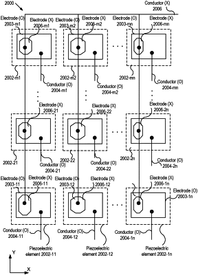
a two-dimensional array of piezoelectric elements, each piezoelectric element including:
a piezoelectric layer;
a bottom electrode disposed on a bottom side of the piezoelectric layer; and
a first top electrode disposed on a top side of the piezoelectric layer; and
an application-specific integrated circuit (ASIC) chip comprising an array of driver circuits for driving the two-dimensional array of piezoelectric elements, each of the driver circuits being electrically coupled to a corresponding piezoelectric element;
wherein the two-dimensional array of piezoelectric elements is arranged into columns of piezoelectric elements, a first column includes a portion of the piezoelectric elements of the two-dimensional array, and the first column is activated by simultaneously turning on a portion of the driver circuits that control the portion of the piezoelectric elements in the first column of the two-dimensional array.
|