| CPC H10K 59/131 (2023.02) [G09G 3/3258 (2013.01); H10K 50/8426 (2023.02); H10K 59/1213 (2023.02); H10K 59/40 (2023.02); H10K 2102/00 (2023.02)] | 20 Claims |
|
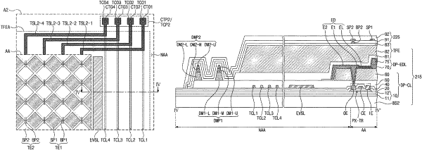
1. A display device comprising:
a base layer having an active area and a peripheral area located outside the active area;
a circuit element layer comprising a pixel circuit located in the active area of the base layer and a driving voltage wiring located in the peripheral area of the base layer to supply a driving voltage to the pixel circuit;
a light emitting element layer comprising a plurality of light emitting elements on the circuit element layer; and
an input sensing layer on the light emitting element layer, the input sensing layer comprising a sensing electrode and a sensing signal wiring part connected to the sensing electrode,
wherein the circuit element layer comprises a connection wiring part located on a same layer as and laterally adjacent to the driving voltage wiring in the peripheral area and being in contact with the sensing signal wiring part.
|