| CPC H10K 59/124 (2023.02) [H10K 50/8426 (2023.02); H10K 59/122 (2023.02); H10K 59/131 (2023.02); H10K 71/00 (2023.02); H10K 59/1201 (2023.02)] | 14 Claims |
|
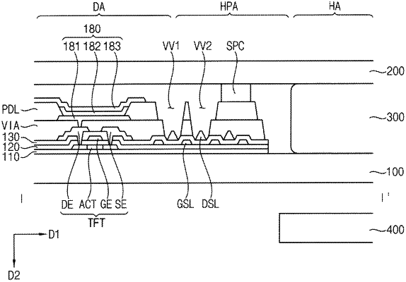
1. A display device comprising:
a base substrate including an opening area, an opening peripheral area, and a display area at least partially surrounding the opening peripheral area, wherein the opening peripheral area is a non-display area at least partially surrounding the opening area;
a thin film transistor disposed on the base substrate in the display area;
a via insulating layer disposed on the thin film transistor and having a first opening surrounding the opening area, wherein the first opening is in the opening peripheral area;
a pixel defining layer disposed on the via insulating layer and having a first opening which overlaps the first opening of the via insulating layer;
a transparent filler disposed on the base substrate in the opening area; and
a sealing substrate disposed on the transparent filler,
wherein the first opening of the pixel defining layer does not overlap the opening area.
|