| CPC H10K 30/82 (2023.02) [H10K 30/353 (2023.02); H10K 39/32 (2023.02); H10K 71/135 (2023.02); H10K 71/164 (2023.02); H10K 71/231 (2023.02)] | 14 Claims |
|
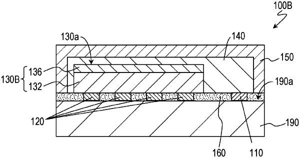
1. A photoelectric conversion element comprising:
a semiconductor substrate having a principal surface;
second electrodes which are located on or above the principal surface, the second electrodes being one- or two-dimensionally arranged;
a photoelectric conversion film covering at least the second electrodes; and
a conductive layer that includes a covering section covering a portion of the photoelectric conversion film, the portion overlapping the second electrodes in plan view, wherein
in a cross section perpendicular to the principal surface, the conductive layer includes an overhanging portion that overhangs a side end portion of the photoelectric conversion film,
in the cross section, an outwardly facing surface of the photoelectric conversion film below the overhanging portion of the conductive layer includes a tapered portion, the tapered portion being located on an outermost side of the photoelectric conversion film, and
in the cross section, a width of the photoelectric conversion film increases toward the principal surface.
|