| CPC H10K 30/10 (2023.02) [H01L 27/14647 (2013.01); H01L 27/14665 (2013.01); H10K 30/81 (2023.02); H10K 39/32 (2023.02); H10K 85/211 (2023.02); H10K 85/636 (2023.02); H10K 85/657 (2023.02); H01L 27/14621 (2013.01); H10K 30/30 (2023.02); H10K 30/57 (2023.02); H10K 85/633 (2023.02); H10K 85/652 (2023.02); H10K 85/6572 (2023.02); H10K 85/6576 (2023.02); H10K 2102/103 (2023.02)] | 21 Claims |
|
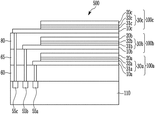
1. A photoelectric device, comprising:
a first electrode;
a second electrode; and
a first photoelectric conversion layer and a second photoelectric conversion layer between the first electrode and the second electrode,
wherein the first photoelectric conversion layer includes a first p-type semiconductor and a first n-type semiconductor to form a first heterojunction,
wherein the second photoelectric conversion layer includes a second p-type semiconductor and a second n-type semiconductor to form a second heterojunction, and
wherein the first photoelectric conversion layer is associated with a first peak absorption wavelength (λmax1), the second photoelectric conversion layer is associated with a second peak absorption wavelength (λmax2), both of the first peak absorption wavelength and the second peak absorption wavelength are included in a common wavelength spectrum of light, the common wavelength spectrum of light being one wavelength spectrum of light of about 410 nm to about 480 nm, about 510 nm to about 560 nm, about 620 nm to about 670 nm, or about 780 nm to about 1200 nm.
|