| CPC H10B 12/37 (2023.02) | 11 Claims |
|
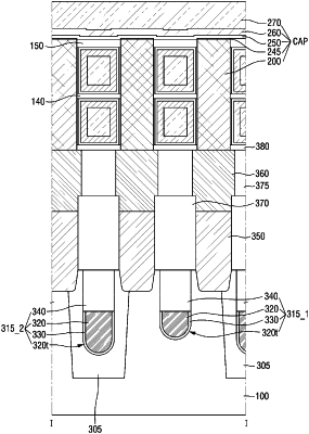
1. A semiconductor device comprising:
a substrate;
a lower electrode on the substrate, the lower electrode including an outer portion and an inner portion that is covered by the outer portion, and the outer portion of the lower electrode including a first region, a second region, and a third region that is between the first region and the second region;
a first supporter pattern on the substrate and contacting the first region of the outer portion of the lower electrode;
a second supporter pattern on the first supporter pattern and contacting the second region of the outer portion of the lower electrode;
a dielectric layer on the third region of the outer portion of the lower electrode;
an insertion layer between the third region of the outer portion of the lower electrode and the dielectric layer; and
an upper electrode on the dielectric layer,
wherein the third region of the outer portion of the lower electrode includes a silicon (Si) dopant,
a concentration of the silicon dopant in the third region of the outer portion of the lower electrode is different from a concentration of the silicon dopant in each of the first region and the second region of the outer portion of the lower electrode, and
the insertion layer includes at least one of niobium oxide, niobium nitride, titanium nitride, titanium oxide, molybdenum nitride, molybdenum oxide, tin nitride, tin oxide, ruthenium, or ruthenium oxide.
|