| CPC H03K 17/6872 (2013.01) [H03K 19/20 (2013.01)] | 20 Claims |
|
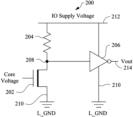
1. A semiconductor device, comprising:
a hysteresis block configured to generate an output voltage at a disabling voltage level and at an enabling voltage level, wherein an input terminal of the hysteresis block is coupled to a control node; and
a core-voltage-gated (CVG) device coupled to the control node, wherein the CVG device is configured to receive a core voltage, the CVG device further being configured to:
alter a control voltage at the control node so as to cause the output voltage of the hysteresis block to be generated at the disabling voltage level in response to the core voltage being at or below a first trigger level; and
alter the control voltage at the control node so as to cause the output voltage of the hysteresis block to be generated at the enabling voltage level in response to the core voltage being at or above a second trigger level, the second trigger level being above the first trigger level; and
one or more resistive devices coupled between a power supply node and the control node, wherein a resistive value is linear and independent of the control voltage at the control node, and there are no non-linear elements between the power supply node and the control node.
|