| CPC H01L 31/1836 (2013.01) [H01L 31/02966 (2013.01); H01L 31/0304 (2013.01); H01L 31/03046 (2013.01); H01L 31/035236 (2013.01); H01L 31/1832 (2013.01); H01L 31/1844 (2013.01); H01L 31/1852 (2013.01); H01L 21/02694 (2013.01); H01L 21/0415 (2013.01); H01L 21/2015 (2013.01)] | 15 Claims |
|
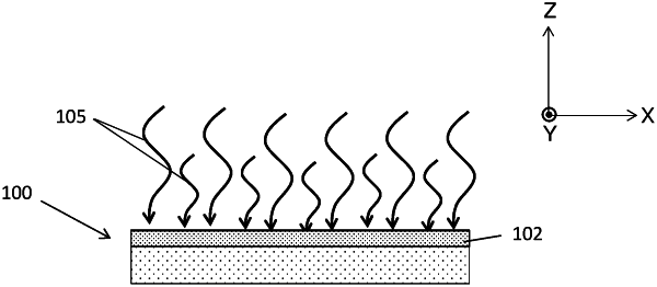
1. A method of fabricating a semiconductor device, the method comprising:
implanting dopants comprising hydrogen (H) into a silicon substrate;
performing a thermal anneal process that activates the implanted dopants, and in response to activating the implanted dopants forming a layer of ultra-thin single-crystal silicon in a portion of the silicon substrate to induce an exfoliation effect that produces a layer of single crystal silicon atop the silicon substrate and accommodates stress and strain into itself while held on top of the silicon substrate; and
performing a heteroepitaxy process to grow a semiconductor material from the layer of ultra-thin single-crystal silicon,
wherein the strain and thickness of the ultra-thin single-crystal silicon accommodate a threading dislocation into the ultra-thin single-crystal silicon, and not into the heteroepitaxially grown semiconductor material so as to reduce the threading dislocations of the heteroepitaxially grown semiconductor material.
|