| CPC H01L 27/14623 (2013.01) [H01L 27/1463 (2013.01); H01L 27/14605 (2013.01); H01L 27/14685 (2013.01); H01L 27/14621 (2013.01); H01L 27/14627 (2013.01)] | 24 Claims |
|
1. A flicker-mitigating pixel-array substrate comprising:
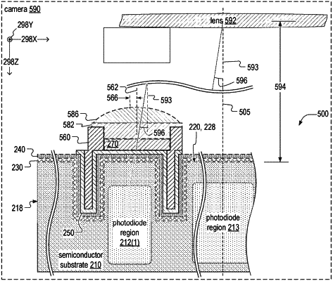
a semiconductor substrate including four large-photodiode regions forming a two-by-two array, and a small-photodiode region located at a center of the two-by-two array, a back surface of the semiconductor substrate forming a trench surrounding the small-photodiode region in a cross-sectional plane parallel to a small back-surface region of the back surface above the small-photodiode region;
a metal annulus at least partially filling the trench, surrounding the small-photodiode region in the cross-sectional plane, extending above the back surface;
a monolithic metal structure including (i) a metal annulus at least partially filling the trench, surrounding the small-photodiode region in the cross-sectional plane and the small back-surface region, extending above the back surface, and (ii) a metal layer covering the small back-surface region; and
a color filter surrounded by the metal annulus and disposed on both the metal annulus and the metal layer.
|