| CPC H01L 27/0886 (2013.01) [H01L 29/0673 (2013.01); H01L 29/0847 (2013.01); H01L 29/26 (2013.01); H01L 29/785 (2013.01)] | 20 Claims |
|
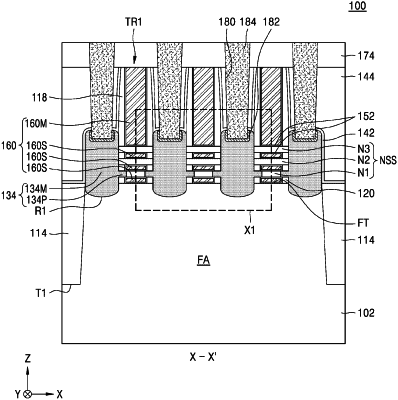
1. An integrated circuit device comprising:
a fin-type active region extending lengthwise in a first direction;
a plurality of nanosheets overlapping each other in a second direction on the fin-type active region, each of the plurality of nanosheets comprising a compound semiconductor layer; and
a source/drain region on the fin-type active region,
wherein the plurality of nanosheets comprises a first nanosheet, which is closest to the fin-type active region, the first nanosheet having a shortest length in the first direction from among the plurality of nanosheets, and
wherein a composition of the compound semiconductor layer in the first nanosheet is different from a composition of the compound semiconductor layer in others of the plurality of nanosheets.
|