| CPC H01L 25/0657 (2013.01) [H01L 21/768 (2013.01); H01L 23/481 (2013.01); H01L 23/4827 (2013.01); H01L 24/05 (2013.01); H01L 25/50 (2013.01)] | 15 Claims |
|
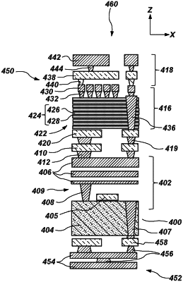
1. A microelectronic device, comprising:
a memory array region comprising:
a stack structure comprising a vertically alternating sequence of conductive structures and insulating structures;
vertically extending strings of memory cells within the stack structure;
conductive line structures vertically overlying the stack structure; and
at least one conductive contact structure vertically extending through the stack structure;
first conductive pad structures underlying the stack structure of the memory array region, the at least one conductive contact structure electrically connected to at least one of the conductive line structures and at least one of the first conductive pad structures;
second conductive pad structures underlying the first conductive pad structures;
a control logic region underlying the second conductive pad structures and comprising control logic devices comprising CMOS circuitry;
additional conductive structures overlying the conductive line structures and in electrical communication with at least some of the conductive line structures; and
bond pad structures overlying and in electrical communication with the additional conductive structures.
|