| CPC H01L 24/24 (2013.01) [H01L 24/05 (2013.01); H01L 24/25 (2013.01); H01L 25/105 (2013.01); H01L 25/18 (2013.01); H01L 23/3107 (2013.01); H01L 23/49822 (2013.01); H01L 24/13 (2013.01); H01L 2224/0401 (2013.01); H01L 2224/13024 (2013.01); H01L 2224/2405 (2013.01); H01L 2224/2413 (2013.01); H01L 2224/24155 (2013.01); H01L 2224/2505 (2013.01); H01L 2224/25171 (2013.01); H01L 2224/25174 (2013.01); H01L 2224/82101 (2013.01); H01L 2224/82106 (2013.01); H01L 2225/1035 (2013.01); H01L 2225/1041 (2013.01); H01L 2225/1058 (2013.01)] | 20 Claims |
|
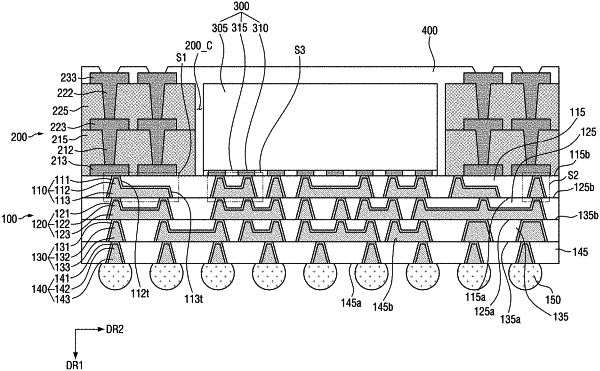
1. A semiconductor package comprising:
an insulating layer including a first face and a second face opposite each other;
a redistribution pattern including a wiring region and a via region in the insulating layer, the wiring region being on the via region; and
a first semiconductor chip connected to the redistribution pattern, the first semiconductor chip being on the redistribution pattern,
an upper face of the wiring region being coplanar with the first face of the insulating layer,
at least one of a first side wall of the redistribution pattern and a second side wall of the redistribution pattern has no step.
|