| CPC H01L 23/49816 (2013.01) [H01L 21/486 (2013.01); H01L 21/4857 (2013.01); H01L 23/49822 (2013.01); H01L 23/49838 (2013.01); H01L 24/13 (2013.01); H01L 24/16 (2013.01); H01L 2224/13147 (2013.01); H01L 2224/16235 (2013.01); H01L 2224/16237 (2013.01); H01L 2224/16238 (2013.01)] | 20 Claims |
|
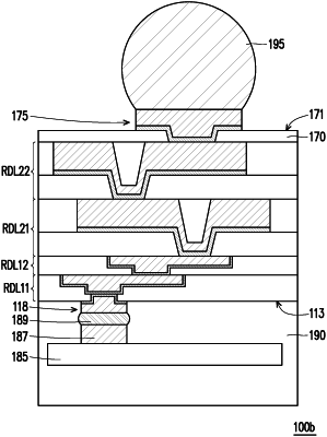
1. A package structure, comprising:
at least one first redistribution layer, comprising a first dielectric layer and a first redistribution circuit, wherein the first dielectric layer comprises a first opening and a second opening communicating with each other, a pore size of the second opening is greater than a pore size of the first opening, the first redistribution circuit fills the first opening and the second opening, and a first upper surface of the first dielectric layer is aligned with a first surface of the first redistribution circuit;
at least one second redistribution layer, disposed on the at least one first redistribution layer, wherein the at least one second redistribution layer comprises a second dielectric layer, a third dielectric layer, and a second redistribution circuit, the second dielectric layer comprises a third opening, the second redistribution circuit is disposed on the second dielectric layer, extends into the third opening, and is electrically connected to the at least one first redistribution layer, the third dielectric layer covers the second dielectric layer and the second redistribution circuit and fills the third opening, and a second upper surface of the third dielectric layer is aligned with a second surface of the second redistribution circuit;
a chip pad, disposed on a first lower surface of the first dielectric layer opposite to the first upper surface, electrically connected to the first redistribution circuit;
a solder ball pad, disposed on the second upper surface of the third dielectric layer, electrically connected to the second redistribution circuit;
a chip, disposed on the chip pad, electrically connected to the chip pad;
a solder ball, disposed on the solder ball pad, electrically connected to the solder ball pad; and
a molding compound, disposed on the first lower surface of the first dielectric layer, at least covering the chip and the chip pad.
|