US 11,710,687 B2
Semiconductor package with guide pin
Chee Hiong Chew, Seremban (MY); Yushuang Yao, Shenzhen (CN); Atapol Prajuckamol, Thanyaburi (TH); and Chuncao Niu, Wuhan (CN)
Assigned to SEMICONDUCTOR COMPONENTS INDUSTRIES, LLC, Scottsdale, AZ (US)
Filed by SEMICONDUCTOR COMPONENTS INDUSTRIES, LLC, Phoenix, AZ (US)
Filed on Jul. 3, 2019, as Appl. No. 16/502,441.
Claims priority of provisional application 62/851,199, filed on May 22, 2019.
Prior Publication US 2020/0373231 A1, Nov. 26, 2020
Int. Cl. H01L 23/498 (2006.01); H05K 1/18 (2006.01); H01L 23/40 (2006.01); H01L 23/538 (2006.01); H01L 23/00 (2006.01)
CPC H01L 23/49811 (2013.01) [H01L 23/40 (2013.01); H01L 23/49838 (2013.01); H01L 23/5385 (2013.01); H01L 23/562 (2013.01); H05K 1/184 (2013.01); H01L 2023/4087 (2013.01)] 18 Claims
OG exemplary drawing
 
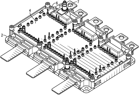
1. A semiconductor package, comprising:
one or more substrates coupled together;
one or more pressfit pins coupled to the one or more substrates; and
two or more guide pins coupled directly on a first side of the one or more substrates;
wherein the two or more guide pins have a height greater than the one or more pressfit pins.