| CPC H01L 23/12 (2013.01) [H01L 23/5384 (2013.01); H01L 23/5385 (2013.01); H01L 23/5386 (2013.01)] | 20 Claims |
|
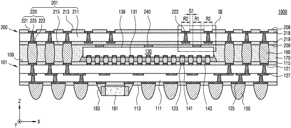
1. A semiconductor package comprising:
a first package substrate;
a first semiconductor chip on the first package substrate;
a first conductive connector on the first package substrate and laterally spaced apart from the first semiconductor chip;
an interposer substrate on the first semiconductor chip and electrically connected to the first package substrate through the first conductive connector, the interposer substrate including a first portion overlapping the first semiconductor chip and a plurality of upper conductive pads in the first portion;
a plurality of spacers on a lower surface of the first portion of the interposer substrate that faces the first semiconductor chip and positioned so as not to overlap the plurality of upper conductive pads in a plan view, the plurality of spacers being in contact with both the interposer substrate and the first semiconductor chip;
an insulating filler between the interposer substrate and the first package substrate, the insulating filler being in contact with the first conductive connector and the first semiconductor chip;
a plurality of second conductive connectors on the plurality of upper conductive pads;
a second package substrate on the plurality of second conductive connectors; and
a second semiconductor chip on the second package substrate.
|