| CPC H01L 21/67271 (2013.01) [H01L 31/186 (2013.01); H01L 33/0095 (2013.01)] | 18 Claims |
|
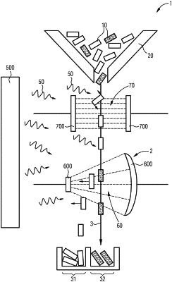
1. A method for sorting optoelectronic semiconductor components each comprising an active region for emission or detection of electromagnetic radiation, comprising the following steps:
introducing the semiconductor components into a sorting region on a specified path,
irradiating the optoelectronic semiconductor components with electromagnetic radiation of a first wavelength range to generate dipole moments by charge separation in the active regions of the optoelectronic semiconductor components, and
deflecting the optoelectronic semiconductor components from the specified path as a function of their dipole moment by means of a non-homogeneous electromagnetic field.
|