| CPC H01L 21/56 (2013.01) [H01L 23/29 (2013.01); H01L 23/3107 (2013.01); H01L 24/92 (2013.01); H01L 2224/92144 (2013.01)] | 15 Claims |
|
12. A fan-out packaging plate, comprising a substrate, and at least one packaging layer made of a thermoplastic material,
wherein one side of the substrate is provided with at least one circuit pattern or at least one electronic part, the substrate and the at least one packaging layer encapsulate the at least one circuit pattern or the at least one electronic part; and alternatively, the substrate is provided with at least one circuit pattern or at least one electronic part, both two sides of the substrate are provided with packaging layers, the packaging layers on the two sides of the substrate encapsulate the substrate, the at least one circuit pattern, and the at least one electronic part,
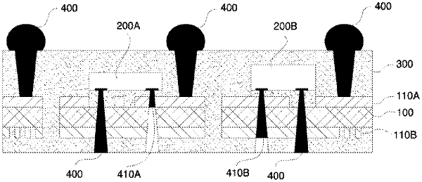
wherein the substrate is provided with at least one via hole, a part of the packaging layers on the two sides of the substrate passes through the at least one via hole, and the packaging layers on the two sides of the substrate are connected with each other through the at least one via hole,
the at least one packaging layer is provided with at least one external connection hole, wherein the at least one external connection hole is butted to a corresponding circuit pattern or a corresponding electronic part, and the at least one external connection hole is provided with an opening in a surface of a corresponding packaging layer; and
wherein at least one interconnection hole is provided in the substrate and the at least one packaging layer, wherein the at least one interconnection hole is provided with an opening on a surface of a corresponding packaging layer, the at least one interconnection hole is butted to a chip and a corresponding circuit pattern, the at least one interconnection hole is provided therein with an interconnection layer, and the chip is electrically connected to the corresponding circuit pattern through the interconnection layer.
|