| CPC H01L 21/0337 (2013.01) [H01L 21/0332 (2013.01); H01L 21/0338 (2013.01); H01L 21/31144 (2013.01)] | 18 Claims |
|
1. A method for fabricating a semiconductor device, the method comprising:
forming an etch mask layer on an etch target layer;
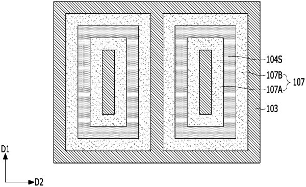
forming a spacer structure in which first spacers and second spacers are alternately disposed and spaced apart from each other on the etch mask layer;
forming first spacer lines through selective etching of the first spacers;
forming second spacer lines through selective etching of the second spacers; and
etching the etch target layer to form a plurality of fine line patterns using the first and second spacer lines,
wherein the forming of the first spacer lines comprises:
forming a first cut mask layer selectively exposing end portions of the first and second spacers on the spacer structure; and
etching an exposed region of the end portions of the first spacers using the first cut mask layer as an etching barrier.
|