| CPC H01L 21/0234 (2013.01) [C23C 16/345 (2013.01); C23C 16/505 (2013.01); H01L 21/0217 (2013.01); H01L 21/02211 (2013.01); H01L 21/02274 (2013.01)] | 20 Claims |
|
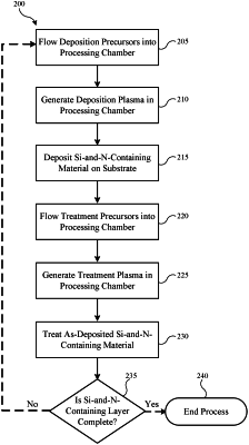
1. A semiconductor processing method comprising:
flowing deposition gases comprising a nitrogen-containing precursor, a silicon-containing precursor, and a carrier gas, into a substrate processing region of a substrate processing chamber, wherein a flow rate ratio of the nitrogen-containing precursor to the silicon-containing precursor is greater than or about 1:1;
generating a deposition plasma from the deposition gases to form a silicon-and-nitrogen-containing layer on a substrate in the substrate processing chamber; and
treating the silicon-and-nitrogen-containing layer with a treatment plasma, wherein the treatment plasma increases a tensile stress of the treated portion of the silicon-and-nitrogen-containing layer, wherein the treatment plasma is formed from the carrier gas without the silicon-containing precursor, and wherein a flow rate of the carrier gas in the treatment plasma is greater than a flow rate of the carrier gas in the deposition plasma.
|