| CPC G06F 30/392 (2020.01) [G03F 1/70 (2013.01); H01L 23/50 (2013.01)] | 20 Claims |
|
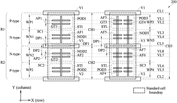
1. A semiconductor device comprising:
a first power rail and a second power rail extending in a row direction;
a third power rail extending in the row direction between the first and second power rails;
a first cell arranged between the first power rail and the second power rail, wherein a cell height of the first cell in a column direction perpendicular to the row direction is equal to a pitch between the first power rail and the second power rail;
a second cell arranged between the first power rail and the third power rail, wherein a cell height of the second cell in the column direction is equal to a pitch between the first power rail and the third power rail; and
a dummy fin structure disposed adjacent to the first cell and the second cell, the dummy fin structure extending in the row direction and overlapped with the third power rail, wherein the dummy fin structure is configured as a non-functional device,
wherein a first active region of the first cell includes a first width in the column direction greater than a second width, in the column direction, of a second active region in the second cell.
|