| CPC G06F 3/0659 (2013.01) [G06F 3/0604 (2013.01); G06F 3/0679 (2013.01); G11C 16/0483 (2013.01); G11C 16/08 (2013.01); G11C 16/24 (2013.01); H10B 41/27 (2023.02); H10B 43/27 (2023.02)] | 14 Claims |
|
1. A nonvolatile memory device comprising:
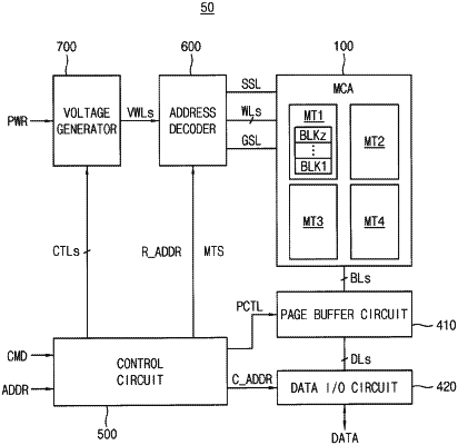
a first semiconductor layer including an upper substrate in which a plurality of word-lines extending in a first direction and a plurality of bit-lines extending in a second direction perpendicular to the first direction are disposed and a memory cell array including a vertical structure on the upper substrate, wherein the vertical structure includes a plurality of memory blocks;
a second semiconductor layer under the first semiconductor layer in a third direction perpendicular to the first and second directions, wherein the second semiconductor layer includes a lower substrate that includes a plurality of address decoders and a plurality of page buffer circuits configured to control the memory cell array;
a control circuit configured to control the plurality of address decoders and the plurality of page buffer circuits in response to a command and an address from an external device; and
a pad region disposed adjacent to the first semiconductor layer in the first direction and extending in the second direction,
wherein the vertical structure includes a plurality of via areas in which one or more through-hole vias are provided and the plurality of via areas are spaced apart in the second direction,
wherein the memory cell array at least includes a first mat and a second mat corresponding to different bit-lines of the plurality of bit-lines,
wherein the first mat is disposed within a reference distance from the pad region in the first direction and the second mat is disposed out of the reference distance from the pad region in the first direction, and
wherein the first mat and the second mat include a different number of the via areas in the first direction.
|