| CPC G02F 1/133514 (2013.01) [H01L 33/502 (2013.01); B82Y 20/00 (2013.01)] | 16 Claims |
|
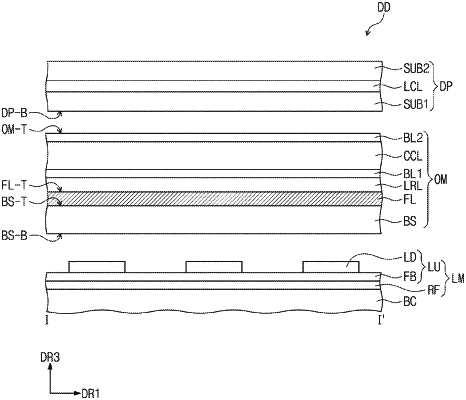
1. A display device comprising:
a light source member including a circuit board and a plurality of light emitting elements disposed on the circuit board and configured to be turned on and off independently of each other;
an optical member disposed on an upper side of the light source member; and
a liquid crystal display panel disposed on an upper side of the optical member,
wherein:
the optical member comprises:
a base substrate;
a color conversion layer disposed on the base substrate and including a quantum dot for converting the first color light into a second color light and a third color light;
a scattering layer disposed on an upper side of the color conversion layer;
a filter layer disposed between the base substrate and the color conversion layer and transmitting the first color light and reflecting the second color light and the third color light; and
an optical path changing layer disposed directly on at least one of an upper surface and a lower surface of the filter layer;
the scattering layer is disposed closer to the liquid crystal display panel than to the color conversion layer; and
the optical path changing layer is a low refraction layer having a refractive index smaller than that of the color conversion layer.
|