| CPC G01R 31/2822 (2013.01) [G01R 27/32 (2013.01); G01R 31/3167 (2013.01)] | 16 Claims |
|
1. A method by a test apparatus for testing a radio frequency (RF) circuit, the method comprising:
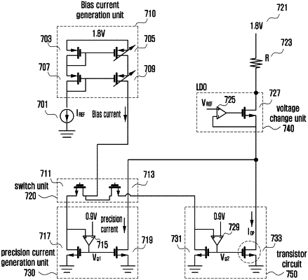
controlling a test circuit of the RF circuit to generate a DC current and identifying a reference resistance by measuring a potential difference between a first end and a second end of a reference resistor;
determining a first drain source current of a transistor circuit based on the reference resistance and a first drain voltage of the transistor circuit, being applied by the test circuit;
determining a second drain source current of the transistor circuit based on the reference resistance and a second drain voltage of the transistor circuit, being applied by the test circuit;
identifying a drain resistance based on the first drain voltage, the second drain voltage, the first drain source current, and the second drain source current; and
performing a test of the RF circuit based on the drain resistance, the first drain source current, and a first threshold value.
|