US 11,708,264 B2
Stacked-die MEMS resonator
Pavan Gupta, Belmont, CA (US); Aaron Partridge, Cupertino, CA (US); and Markus Lutz, Mountain View, CA (US)
Assigned to SiTime Corporation, Santa Clara, CA (US)
Filed by SiTime Corporation, Santa Clara, CA (US)
Filed on May 27, 2022, as Appl. No. 17/827,437.
Application 17/827,437 is a division of application No. 17/143,119, filed on Jan. 6, 2021, granted, now 11,370,656.
Application 17/143,119 is a division of application No. 16/903,116, filed on Jun. 16, 2020, granted, now 10,913,655, issued on Feb. 9, 2021.
Application 16/903,116 is a division of application No. 16/372,745, filed on Apr. 2, 2019, granted, now 10,723,617, issued on Jul. 28, 2020.
Application 16/372,745 is a division of application No. 15/805,031, filed on Nov. 6, 2017, granted, now 10,287,162, issued on May 14, 2019.
Application 15/805,031 is a division of application No. 15/187,748, filed on Jun. 20, 2016, granted, now 9,821,998, issued on Nov. 21, 2017.
Application 15/187,748 is a division of application No. 14/597,825, filed on Jan. 15, 2015, granted, now 9,371,221, issued on Jun. 21, 2016.
Application 14/597,825 is a division of application No. 14/191,978, filed on Feb. 27, 2014, granted, now 8,941,247, issued on Jan. 27, 2015.
Application 14/191,978 is a division of application No. 13/681,065, filed on Nov. 19, 2012, granted, now 8,669,664, issued on Mar. 11, 2014.
Application 13/681,065 is a division of application No. 13/151,316, filed on Jun. 2, 2011, granted, now 8,324,729, issued on Dec. 4, 2012.
Application 13/151,316 is a division of application No. 11/763,801, filed on Jun. 15, 2007, granted, now 8,022,554, issued on Sep. 20, 2011.
Claims priority of provisional application 60/813,874, filed on Jun. 15, 2006.
Prior Publication US 2022/0356059 A1, Nov. 10, 2022
This patent is subject to a terminal disclaimer.
Int. Cl. B81B 7/00 (2006.01); B81C 1/00 (2006.01); H10N 30/30 (2023.01); H01L 23/34 (2006.01); H01L 23/498 (2006.01); H01L 23/31 (2006.01)
CPC B81B 7/0083 (2013.01) [B81B 7/007 (2013.01); B81B 7/0077 (2013.01); B81C 1/0023 (2013.01); B81C 1/00301 (2013.01); B81C 1/00333 (2013.01); B81C 1/00341 (2013.01); H01L 23/34 (2013.01); H01L 23/498 (2013.01); H10N 30/302 (2023.02); B81B 2201/0271 (2013.01); B81B 2207/07 (2013.01); B81B 2207/094 (2013.01); B81C 2201/016 (2013.01); B81C 2203/0118 (2013.01); B81C 2203/0154 (2013.01); H01L 23/3107 (2013.01); H01L 2224/48091 (2013.01); H01L 2224/48245 (2013.01); H01L 2224/48247 (2013.01); H01L 2224/73265 (2013.01); H01L 2924/01019 (2013.01); H01L 2924/10253 (2013.01); H01L 2924/1461 (2013.01); H01L 2924/181 (2013.01)] 20 Claims
OG exemplary drawing
 
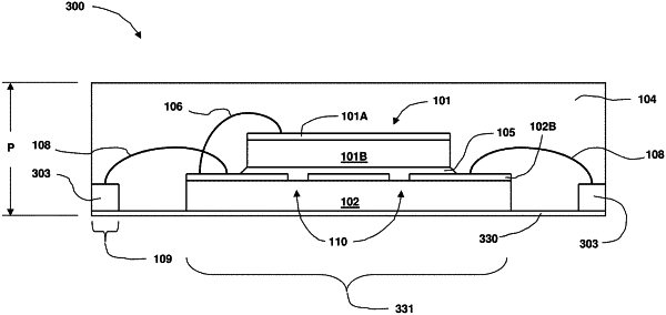
1. An integrated circuit comprising:
a first die having a microelectromechanical system (MEMS) resonator;
a second die having complementary metal oxide semiconductor (CMOS) circuitry;
wherein the first die and the second die are stacked together and are directly electrically interconnected by at least one of wire bonds or solder bumps;
one or more metallic structures on an exterior surface of the integrated circuit, the one or more metaling structures being in electrical communication with the CMOS circuitry;
encapsulation of the first die and the at least one of the wirebonds or solder bumps, relative to the second die, that seals the first die from an atmosphere external to the integrated circuit;
wherein the one or more metallic structures are to electrically connect the integrated circuit with external electronics.