| CPC H10N 60/01 (2023.02) [G06N 10/00 (2019.01); H10N 60/128 (2023.02); H10N 60/84 (2023.02)] | 15 Claims |
|
1. A method for fabricating a quantum device, the method comprising:
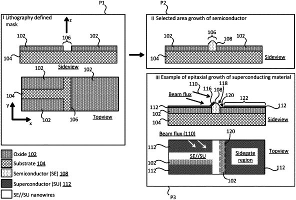
providing a substrate and an insulator formed on the substrate;
from combinations of selective-area-grown semiconductor material along with regions of a superconducting material, forming a network of nanowires oriented in a plane of the substrate that is gateable to produce a Majorana-based topological qubit; and
fabricating a side gate for controlling a topological segment of the Majorana-based topological qubit;
wherein the selective-area-grown semiconductor material is grown on the substrate by etching trenches in the insulator formed on the substrate to define the nanowires and depositing the semiconductor material in the trenches defining the nanowires; and
wherein the fabricating of the side gate comprises etching the insulator to create a trench for the side gate and depositing the side gate in the trench for the side gate.
|