| CPC H10K 50/818 (2023.02) [H10K 50/852 (2023.02); H10K 50/856 (2023.02); H10K 71/00 (2023.02)] | 26 Claims |
|
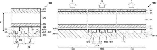
1. A light emitting device comprising:
a reflective layer comprising a plurality of nanostructures that are periodically two-dimensionally arranged;
a planarization layer disposed on the reflective layer;
a first electrode disposed on the planarization layer;
an organic emission layer disposed on the first electrode; and
a second electrode disposed on the organic emission layer,
wherein the planarization layer comprises a conductive material that is transparent with respect to light emitted by the organic emission layer,
wherein the planarization layer is disposed on upper surfaces of the plurality of nanostructures such that an air gap is provided between adjacent nanostructures of the plurality of nanostructures, and
wherein the planarization layer further comprises an organic-inorganic hybrid layer in which reduced graphene oxide is dispersed.
|