| CPC H10K 50/11 (2023.02) [H10K 50/15 (2023.02); H10K 50/156 (2023.02); H10K 50/16 (2023.02); H10K 50/171 (2023.02); H10K 2101/30 (2023.02); H10K 2101/40 (2023.02)] | 11 Claims |
|
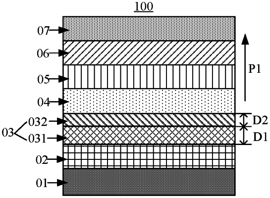
1. An electroluminescent device, comprising a hole inject layer, a hole transport layer, an electroluminescent layer, an electron transport layer, and an electron inject layer,
wherein at least one of the hole inject layer, the hole transport layer, the electron transport layer, and the electron inject layer is a target film comprising a small molecular layer with a small molecule and a large molecular layer with a large molecule which are arranged in a stacked manner, and
wherein the large molecular layer of the target film is closer to the electroluminescent layer than the small molecular layer of the target film, and the large molecular layer has a cross-linked network structure
wherein a relative molecular mass of the large molecule of the large molecular layer ranges from several thousands to several millions, and a relative molecular mass of the small molecule of the small molecular layer is smaller than five hundreds, and
wherein the small molecular layer has a thickness larger than that of the large molecular layer.
|
|
10. A method for fabricating an electroluminescent device, comprising:
forming an electroluminescent device on a substrate, wherein the electroluminescent device comprises a hole inject layer, a hole transport layer, an electroluminescent layer, an electron transport layer, and an electron inject layer,
wherein at least one of the hole inject layer, the hole transport layer, the electron transport layer, and the electron inject layer is a target film comprising a small molecular layer with a small molecule and a large molecular layer with a large molecule which are arranged in a stacked manner, and
wherein the large molecular layer of the target film is closer to the electroluminescent layer than the small molecular layer of the target film, and the large molecular layer has a cross-linked network structure,
wherein a relative molecular mass of the large molecule of the large molecular layer ranges from several thousands to several millions, and a relative molecular mass of the small molecule of the small molecular layer is smaller than five hundreds, and
wherein the small molecular layer has a thickness larger than that of the large molecular layer.
|