| CPC H10B 43/27 (2023.02) [H10B 41/27 (2023.02); H10B 41/35 (2023.02); H10B 41/41 (2023.02); H10B 43/35 (2023.02); H10B 43/40 (2023.02)] | 20 Claims |
|
1. A method of forming a semiconductor device, the method comprising:
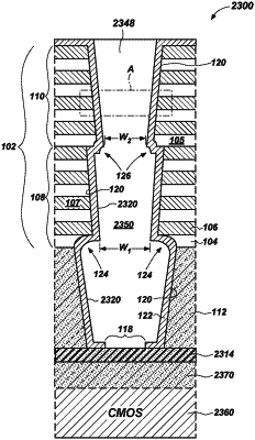
forming a stack of vertically-alternating tiers of insulative material and other material over a base material, a sacrificial material disposed in the base material, and a soft plug material disposed in the sacrificial material;
forming an opening extending through the stack and through the soft plug material, leaving remnants of the soft plug material along sidewalls of the opening;
forming a liner in the opening;
exposing, through the liner, a portion of the sacrificial material;
without removing the liner, removing the sacrificial material and the remnants of the soft plug material to define a gap between the liner and a sidewall of the base material, the gap exposing a portion of a lower tier of the stack;
etching into the portion of the lower tier of the stack to define an undercut portion in the lower tier of the stack; and
removing the liner to form a channel opening extending through the stack and into the base material, the channel opening exposing a source region of the base material at a base of the channel opening, the channel opening defined by sidewalls comprising the undercut portion.
|
|
7. A method of forming a semiconductor device, the method comprising:
forming a first deck of vertically-alternating tiers of insulative material and other material over a base material and a sacrificial material disposed in the base material;
forming an opening extending through the first deck and into the sacrificial material;
forming a liner and a fill material within the opening;
forming a second deck of vertically-alternating tiers of the insulative material and the other material over the first deck, the liner, and the fill material;
forming another opening extending through the second deck to the fill material within the opening;
forming another liner within the other opening;
exposing a portion of the fill material through the other liner;
without removing the liner or the other liner, removing the fill material and the sacrificial material to form an extended opening exposing at least a portion of a lower tier of each of the first deck and the second deck;
isotropically etching the portion of the lower tier of each of the first deck and the second deck to define undercut portions; and
removing the liner and the other liner to form a channel opening defined by sidewalls comprising the undercut portions.
|
|
10. A method of forming an electronic device, comprising:
forming a deck above at least one sacrificial material, the deck comprising insulative structures vertically alternating with other structures and arranged in tiers;
forming an opening through the deck and to or into the at least one sacrificial material;
forming a liner in the opening along sidewalls of the deck;
without substantially removing sidewalls of the liner, removing at least a portion of the at least one sacrificial material to expose a portion of a lower surface of a lowest insulative structure of the insulative structures of the deck;
etching into the portion of the lower surface of the lowest insulative structure of the insulative structures of the deck; and
removing the liner to form a channel opening tapering through the tiers of the deck above the lowest insulative structure, the channel opening broadening at the lowest insulative structure.
|