| CPC H10B 43/27 (2023.02) [G11C 7/18 (2013.01); H01L 24/46 (2013.01); H10B 41/10 (2023.02); H10B 41/27 (2023.02); H10B 41/35 (2023.02); H10B 43/10 (2023.02); H10B 43/35 (2023.02)] | 16 Claims |
|
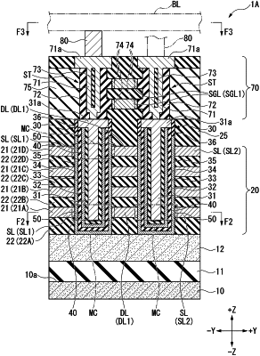
1. A semiconductor storage device comprising:
a substrate having a surface;
a first source line extending in a first direction along the surface;
a first drain line aligned with the first source line in a second direction and extending in the first direction, the second direction intersecting with the first direction;
a first channel portion in contact with the first source line and the first drain line, the first channel portion including a semiconductor;
a first gate wiring located between the first source line and the first drain line, the first gate wiring extending in a third direction intersecting with the first direction and the second direction, the first gate wiring aligned with the first channel portion in the first direction; and
a first charge storage located between the first channel portion and the first gate wiring.
|