| CPC H10B 12/31 (2023.02) [H01L 23/5283 (2013.01); H10B 12/033 (2023.02); H10B 12/05 (2023.02); H10B 12/488 (2023.02)] | 24 Claims |
|
1. An assembly, comprising:
a semiconductor material having a horizontal surface;
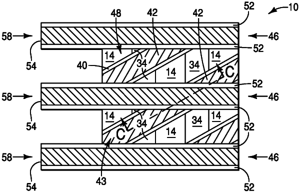
a row of vertically-extending semiconductor pillars over the horizontal surface; each of the semiconductor pillars comprising a transistor channel region vertically disposed between a first source/drain region and a second source/drain region;
a wordline extending along the row of vertically-extending semiconductor pillars, and being adjacent to the transistor channel regions of the semiconductor pillars; the wordline having a first lateral surface and an opposing second lateral surface; the semiconductor pillars being subdivided amongst a first set along the first lateral surface, and a second set along the second lateral surface; the semiconductor pillars of the first set alternating with the semiconductor pillars of the second set along the row;
a gate dielectric material between the first lateral surface and the transistor channel regions of the semiconductor pillars of the first set, and between the second lateral surface and the transistor channel regions of the semiconductor pillars of the second set;
a conductive shield material between the semiconductor pillars of the first set, and between the semiconductor pillars of the second set;
bitlines coupled with the first source/drain regions; and
storage elements coupled with the second source/drain regions.
|