| CPC H05K 5/0091 (2013.01) [H01L 24/72 (2013.01); H01L 25/072 (2013.01); H05K 5/06 (2013.01)] | 11 Claims |
|
1. A method for arranging a power semiconductor module, on a motor which comprises a motor contact device, comprising the steps of:
a) providing said power semiconductor module, said power semiconductor module further comprising:
a power semiconductor assembly having a housing which, in a housing side with an outer surface, has a recess with a direction of passage in a normal direction (N) of said outer surface;
an internal contact device, which has an electrically conducting contact inside the housing to an external connection element, designed as a load terminal element, with one section arranged in the recess, and having a spring element;
the external connection element is designed as a rigid metallic shaped body with an inner and an outer contact surface;
wherein the outer contact surface is accessible from the outside;
the external connection element is connected to the housing via an electrically insulating and mechanically elastic retaining device such that said external connection element is moveable in a direction of the recess;
wherein the spring element is arranged and designed in such a way that a spring action of the spring element acts directly or indirectly on the external connection element in the direction of the recess;
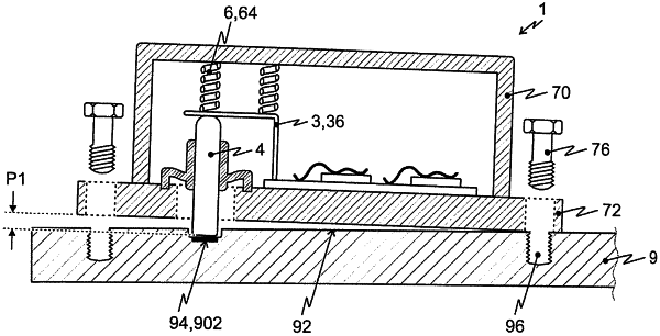
wherein the external connection element has a first connection element position relative to the direction of passage, in which the outer contact surface relative to the outer surface has a first contact surface position (P1);
wherein the external connection element can be displaced in a negative direction (N) of passage against a spring force of the spring element;
wherein the first contact surface position (P1) is recessed in the direction of passage in relation to the outer surface, or is formed flush with the outer surface or protrudes through the outer surface; and
wherein the spring element is designed to press on the internal contact device) on the inner contact surface of the external connection element in the direction of passage and wherein the internal contact device is arranged between the spring element and the external connection element for this purpose;
b) deploying the power semiconductor module, wherein the outer contact surface is located relative to the outer surface of the housing side of the housing of the power semiconductor module in the first contact surface position (P1);
c) arranging the power semiconductor module with respect to a power module surface of the motor, in such a way that the outer contact surface of the external connection element of the power semiconductor module comes to rest on the motor contact device associated with said outer contact surface, wherein the outer contact surface remains in the first contact surface position (P1) relative to the outer surface; and
d) fixing the power semiconductor module with the outer surface thereof on the power module surface by means of a mounting device, wherein the outer contact surface is displaced in the negative direction (N) of passage from the first contact surface position (P1) into a second contact surface position (P2), as a result of which an electrically conducting pressure contact generated by the spring element of the power semiconductor module is formed between the outer contact surface and the associated motor contact device.
|