| CPC H05K 3/3463 (2013.01) [H01L 23/49811 (2013.01); H01L 23/49822 (2013.01); H05K 1/113 (2013.01); H05K 3/4644 (2013.01)] | 14 Claims |
|
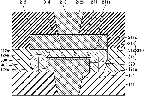
1. A composite wiring substrate comprising:
a first wiring substrate including a first connection terminal;
a second wiring substrate including a second connection terminal facing the first connection terminal; and
a joint material joining the first connection terminal and the second connection terminal,
wherein a first outline of the first connection terminal is inside a second outline of the second connection terminal in a plan view, and
the joint material includes
a first portion famed of an intermetallic alloy of copper and tin, and contacting each of the first connection terminal and the second connection terminal, and
a second portion formed of an alloy of tin and bismuth, and including a portion between the first outline and the second outline in the plan view, the second portion containing the bismuth at a higher concentration than in a eutectic composition of a tin-bismuth alloy, the second portion being separated from the second connection terminal.
|