| CPC H04B 10/80 (2013.01) [G02B 6/4249 (2013.01); G02B 6/4274 (2013.01); G11C 5/04 (2013.01); G11C 5/06 (2013.01); G11C 5/141 (2013.01); G11C 11/42 (2013.01); H04B 10/516 (2013.01)] | 18 Claims |

|
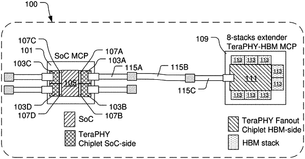
1. A computer memory system, comprising:
a plurality of memory devices;
an electro-optical chip including an electrical interface and a photonic interface, the photonic interface configured to optically connect with an optical link, the electro-optical chip including an optical macro, the optical macro configured to convert outgoing electrical data signals received through the electrical interface into outgoing optical data signals, the optical macro configured to transmit the outgoing optical data signals through the photonic interface to the optical link, the optical macro configured to convert incoming optical data signals received through the photonic interface from the optical link into incoming electrical data signals, the optical macro configured to transmit the incoming electrical data signals through the electrical interface, wherein the optical macro includes a transmitter slice that includes an optical microring resonator configured to modulate light signals of a particular wavelength in accordance with electrical data signals, and wherein the optical macro includes a receiver slice that includes another optical microring resonator configured to optically in-couple light signals of another particular wavelength; and
an electrical circuit configured to direct transmission of data communication signals between the electrical interface of the electro-optical chip and each of the plurality of memory devices.
|