| CPC H04B 10/03 (2013.01) [H04B 10/27 (2013.01)] | 3 Claims |
|
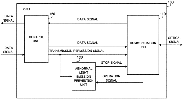
1. An optical communication device as a slave station device that communicates with a master station device, comprising:
a communicating circuitry;
an abnormal light emission preventing circuitry; and
a controlling circuitry to transmit a data signal and a transmission permission signal to the communicating circuitry and to transmit the transmission permission signal to the abnormal light emission preventing circuitry for a time period between a transmission start time and a transmission end time based on transmission band assignment information as information regarding transmission of an optical signal, wherein
when the transmission permission signal is received, the communicating circuitry transduces the data signal into an optical signal, transmits the transduced optical signal to the master station device, and transmits an operation signal indicating that the communicating circuitry is operating to the abnormal light emission preventing circuitry during the transmission of the transduced optical signal,
the abnormal light emission preventing circuitry transmits a stop signal to the communicating circuitry when a difference between a time for which the transmission permission signal is received and a time for which the operation signal is received is greater than or equal to a predetermined threshold value, and
the communicating circuitry stops when the stop signal is received.
|