| CPC H04B 1/0483 (2013.01) [H04B 1/0475 (2013.01); H04B 1/10 (2013.01); H04B 2001/0491 (2013.01)] | 20 Claims |
|
1. An apparatus for receiving radio frequency (RF) signals, comprising:
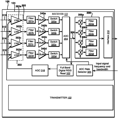
a receive path for receiving receive signals, the receive path including a plurality of input signal ports, the plurality of input signal ports corresponding to a plurality of receive path segments, each receive path segment being coupled to a variable rate analog-to-digital converter (ADC),
a first receive path segment including,
a first low noise amplifier (LNA) and a first switch component configured to receive a first receive signal associated with a first frequency range and a first bandwidth,
wherein when the variable rate ADC is electrically coupled with the first switch component, the variable rate ADC operates at a first sampling rate that is assigned based on the first frequency range and the first bandwidth and generates a first digital signal, and
a second receive path segment including,
a second LNA and a second switch component configured to receive a second receive signal associated with a second frequency range and a second bandwidth,
wherein when the variable rate ADC is electrically coupled with the second switch component, the variable rate ADC operates at a second sampling rate that is assigned based on the second frequency range and the second bandwidth and generates a second digital signal, and
wherein the first receive path segment and the second receive path segment are provided on a single die, and wherein a first gain of the first LNA and a second gain of the second LNA is based on an output of the variable rate ADC.
|