| CPC H01S 5/2031 (2013.01) [H01S 5/0424 (2013.01); H01S 5/0651 (2013.01); H01S 5/1032 (2013.01); H01S 5/12 (2013.01); H01S 5/2018 (2013.01); H01S 5/2022 (2013.01); H01S 5/2027 (2013.01); G02B 6/0281 (2013.01); H01S 5/223 (2013.01); H01S 2301/16 (2013.01)] | 20 Claims |
|
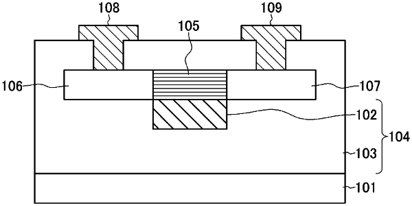
1. A semiconductor optical device comprising:
an optical waveguide on a substrate, the optical waveguide including a core having a thickness at which a higher-order mode appears;
an active layer above the substrate, the active layer extending along the core and configured to be optically coupled to the core, wherein the core and the active layer are in physical contact with each other;
a p-type semiconductor layer and an n-type semiconductor layer in contact with the active layer above the substrate and sandwiching the active layer in a plan view; and
a resonator structure configured to confine light in the active layer.
|