| CPC H01Q 21/0087 (2013.01) [H01Q 1/38 (2013.01); H01Q 3/26 (2013.01); H01Q 21/0025 (2013.01)] | 29 Claims |
|
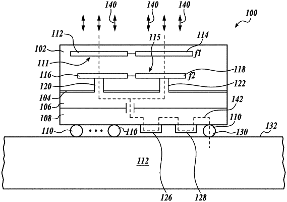
1. An apparatus comprising:
a plurality of conductive structures having first sides and second sides opposite the first sides, wherein the second sides of the plurality of conductive structures are configured to be physically coupleable with a printed circuit board (PCB) of a receiver or a transmitter, and wherein the first sides of the plurality of conductive structures are configured to be spaced from the PCB by a first distance when the plurality of conductive structures is physically coupled with the PCB; and
an antenna having a first side and a second side opposite the first side, wherein the first side comprises a radiating side of the antenna and the second side of the antenna is disposed closer to the plurality of conductive structures than the first side of the antenna when the plurality of conductive structures is physically coupled with the PCB.
|