| CPC H01P 5/02 (2013.01) [H01P 1/047 (2013.01); H01P 3/026 (2013.01); H01P 3/16 (2013.01); H01P 5/028 (2013.01); H01P 5/107 (2013.01)] | 21 Claims |
|
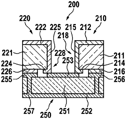
1. A waveguide structure comprising:
at least one first waveguide section mechanically and electrically connected by at least one fixed connector to at least one second waveguide section,
wherein each of the at least one first waveguide section and the at least one second waveguide section comprises:
at least one layer of a first dielectric material having respective first layer top side, first layer bottom side, and two first layer opposing ends,
a ground layer of a corresponding first electrically conductive material on the first layer bottom side,
at least one conductor structure including a pair of elongated conductors of a corresponding second electrically conductive material on the first layer top side,
the at least one conductor structure being insulated from the ground layer, and
an interface section at at least one of the two first layer opposing ends;
wherein the at least one fixed connector comprises:
at least one layer of a second dielectric material having respective second layer top side, second layer bottom side, and two second layer opposing ends,
at least one pair of contact pads of a corresponding third electrically conductive material on the top side, and
a connector ground layer of a corresponding fourth electrically conductive material on the second layer top side and insulated from the at least one pair of contact pads,
wherein the at least one fixed connector is attached by a top side thereof
to a bottom side of an interface section of a first end of the at least one first waveguide section, having a respectively corresponding electrical contact between the connector ground layer and a ground layer of the at least one first waveguide section,
to the bottom side of an interface section of a second end of the at least one second waveguide section, having a respectively corresponding electrical contact between the connector ground layer and a ground layer of the at least one second waveguide section,
wherein:
each of the interface sections of the at least one first waveguide section and the at least one second waveguide section comprises a corresponding intermediate conductor extending from each of elongated conductors at the first layer top side to the first layer bottom side of the at least one layer of the first dielectric material,
each of said corresponding intermediate conductors is connected to one of the at least one pair of contact pads and insulated from the corresponding ground layer of the at least one of the first waveguide section and the at least one second waveguide section,
the at least one first and the at least one second waveguide sections are opposing each other and at least one intermediate conductor of the first waveguide section is connected to a corresponding intermediate conductor of the opposing second waveguide section by the at least one pair of contact pads.
|