| CPC H01L 33/007 (2013.01) [H01L 25/0753 (2013.01); H01L 33/0093 (2020.05); H01L 33/0095 (2013.01); H01L 2933/005 (2013.01); H01L 2933/0016 (2013.01); H01L 2933/0025 (2013.01); H01L 2933/0066 (2013.01)] | 19 Claims |
|
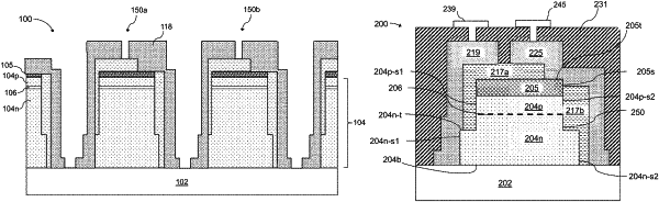
1. A method of manufacturing a micro-light emitting diode (uLED) device comprising:
depositing a plurality of semiconductor layers including an n-type layer, an active layer, and a p-type layer on a substrate;
depositing a p-contact layer on the plurality of semiconductor layers;
depositing a hard mask layer on the p-contact layer;
etching a portion of the semiconductor layers, the p-contact layer, and the hard mask layer to form trenches and plurality of mesas, each of the mesas having a height spanning from a top surface of the p-contact layer to a bottom surface of the n-type layer and a width spanning a first sidewall of the n-type layer to a second sidewall of the n-type layer;
depositing a dielectric metal over the substrate into the trenches and on an uppermost surface of the substrate;
first etching to expose the p-contact layer and a first portion of a surface of the substrate;
second etching to expose the n-type layer and a second portion of the surface of the substrate;
depositing a first metal onto areas exposed by the first etching and the second etching; and
etching to form a cathode and an anode which are isolated from each other;
the foregoing steps forming a processed structure.
|