| CPC H01L 31/0376 (2013.01) [H01L 27/14647 (2013.01); H01L 31/032 (2013.01); H01L 31/102 (2013.01)] | 14 Claims |
|
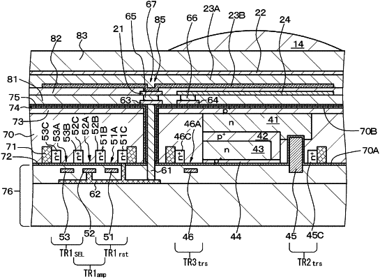
1. An imaging device comprising:
a photoelectric conversion unit in which a first electrode, a photoelectric conversion layer, and a second electrode are stacked; and
a semiconductor material layer including an inorganic oxide semiconductor material between the first electrode and the photoelectric conversion layer,
wherein at least a portion of the inorganic oxide semiconductor material has a crystalline structure with a formation energy having a positive value in units of eV/atom,
wherein the inorganic oxide semiconductor material includes Gax1Sny1O, and satisfies 0.28≤[y1/(x1+y1)]≤0.38, and
wherein the inorganic oxide semiconductor material has an amorphous structure in at least one portion.
|