| CPC H01L 29/78618 (2013.01) [H01L 29/45 (2013.01); H01L 29/66969 (2013.01); H01L 29/7869 (2013.01); H01L 29/78696 (2013.01)] | 4 Claims |
|
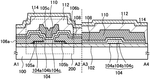
1. A semiconductor device comprising:
a first oxide film;
an oxide semiconductor film over the first oxide film;
a source electrode and a drain electrode, each having a region in contact with a top surface and a side surface of the oxide semiconductor film;
a second oxide film over the source electrode and the drain electrode, the second oxide film having a region in contact with the top surface of the oxide semiconductor film;
a gate insulating film over the second oxide film; and
a gate electrode over the gate insulating film,
wherein the oxide semiconductor film has a first low-resistance region between the source electrode and the oxide semiconductor film, and a second low-resistance region between the drain electrode and the oxide semiconductor film, and
wherein an end portion of the oxide semiconductor film has a larger taper angle than an end portion of the first oxide film.
|