| CPC H01L 29/7816 (2013.01) [H01L 29/0653 (2013.01); H01L 29/0692 (2013.01); H01L 29/0847 (2013.01); H01L 29/0869 (2013.01); H01L 29/0886 (2013.01); H01L 29/1095 (2013.01); H01L 29/78 (2013.01)] | 13 Claims |
|
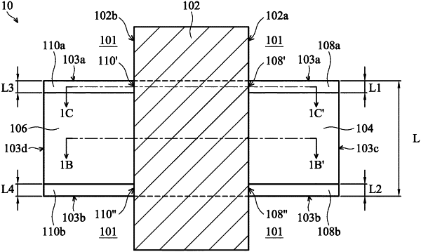
1. A MOS transistor for power integrated circuits (ICs), comprising:
a semiconductor substrate having an active area, wherein the active area has a first edge and a second edge opposite thereto;
a gate layer disposed on the active area of the semiconductor substrate and having a first edge and a second edge opposite thereto, extending across the first and second edges of the active area;
first and second heavily doped regions of a first conductivity type in the active area at opposite sides of the gate layer and between the first and second edges of the active area; and
first and second heavily doped regions of a second conductivity type in the active area directly physically contacting the first and second heavily doped regions of the first conductivity type respectively, wherein
the first and second heavily doped regions of the second conductivity type have respective edges, and
the edges of the first and second heavily doped regions of the second conductivity type are coplanar with the first and second edges of the gate layer respectively.
|