| CPC H01L 29/42392 (2013.01) [H01L 29/0673 (2013.01); H01L 29/512 (2013.01); H01L 29/78696 (2013.01)] | 22 Claims |
|
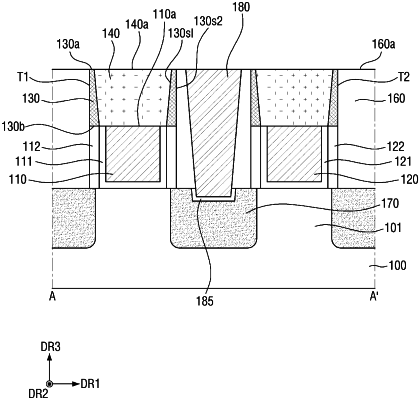
1. A semiconductor device comprising:
a substrate;
an active pattern extending in a first direction on the substrate;
a gate electrode extending in a second direction on the active pattern, the second direction intersecting the first direction;
a gate spacer extending in the second direction along side walls of the gate electrode;
an interlayer insulating layer contacting side walls of the gate spacer;
a trench formed on the gate electrode in the interlayer insulating layer;
a first capping pattern provided along side walls of the trench, at least one side wall of the first capping pattern having an inclined profile, wherein the first capping pattern decreases in width with increased distance from the substrate, a first side wall of the at least one side wall is in contact with a second capping pattern, and the first capping pattern is not in contact with the gate electrode; and
the second capping pattern provided on the first capping pattern in the trench.
|