| CPC H01L 29/0634 (2013.01) [H01L 29/0653 (2013.01); H01L 29/1095 (2013.01); H01L 29/404 (2013.01); H01L 29/7816 (2013.01); H01L 29/7819 (2013.01); H02M 3/158 (2013.01)] | 7 Claims |
|
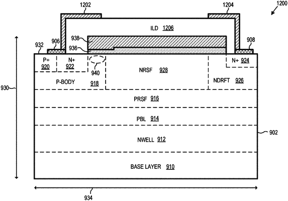
1. A lateral double-diffused metal-oxide-semiconductor (LDMOS) transistor including a breakdown voltage clamp, comprising:
a drain n+ region;
a source n+ region;
a gate;
an n-type reduced surface field (NRSF) layer disposed between the source n+ region and the drain n+ region in a lateral direction;
a p-type reduced surface field (PRSF) layer disposed below the NRSF layer in a thickness direction orthogonal to the lateral direction;
a p-type buried layer (PBL) disposed below the PRSF layer in the thickness direction, the drain n+ region being disposed over the PBL in the thickness direction; and
an n-type drift (NDRFT) region disposed over the PRSF layer and adjacent to the NRSF layer in the lateral direction, wherein the drain n+ region is disposed in the NDRFT region.
|