| CPC H01L 27/14645 (2013.01) [H01L 27/14612 (2013.01); H01L 27/14629 (2013.01); H01L 27/14621 (2013.01); H01L 27/14627 (2013.01)] | 20 Claims |
|
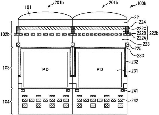
1. A light detecting device, comprising:
a semiconductor substrate including a first photoelectric conversion region and a second photoelectric conversion region;
a first separation region disposed in the semiconductor substrate, wherein the first separation region is disposed between the first photoelectric conversion region and the second photoelectric conversion region in a cross-sectional view; and
an optical filter disposed above a light-receiving surface of the semiconductor substrate,
wherein the optical filter comprises:
a diffraction grating;
a first core layer; and
a first portion of a reflector disposed above the first separation region in the cross-sectional view,
wherein a refractive index of the reflector is different from a refractive index of the first core layer.
|