| CPC H01L 27/14634 (2013.01) [H01L 24/16 (2013.01); H01L 24/32 (2013.01); H01L 24/83 (2013.01); H01L 24/92 (2013.01); H01L 27/1469 (2013.01); H01L 27/14636 (2013.01); H01L 2224/08145 (2013.01); H01L 2224/16145 (2013.01); H01L 2224/16146 (2013.01); H01L 2224/16505 (2013.01); H01L 2224/32145 (2013.01); H01L 2224/80895 (2013.01); H01L 2224/83896 (2013.01); H01L 2224/9201 (2013.01); H01L 2224/92143 (2013.01); H01L 2224/92242 (2013.01)] | 12 Claims |
|
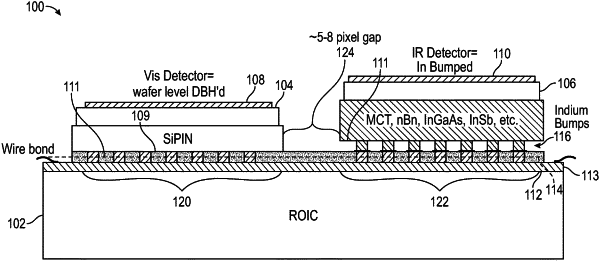
1. A semiconductor-based imaging device, comprising:
a silicon-based support structure having a bonding surface with a first bonding location and a second bonding location;
a first direct bond hybridization (DBH) structure on the bonding surface extending from the first bonding location to the second bonding location;
a first detector formed on a silicon layer;
a second DBH structure between the silicon layer of the first detector and the first DBH structure of the silicon-based support structure at the first bonding location;
a second detector formed on a non-silicon layer; and
an indium-bump layer between the non-silicon layer of the second detector and the first DBH structure of the silicon-based support structure at the second bonding location.
|