| CPC H01L 27/124 (2013.01) [H01L 27/1262 (2013.01); H10K 59/131 (2023.02)] | 21 Claims |
|
1. An electronic device comprising:
a panel including at least one transistor; and
a driving circuit driving the panel,
wherein the panel includes:
a substrate;
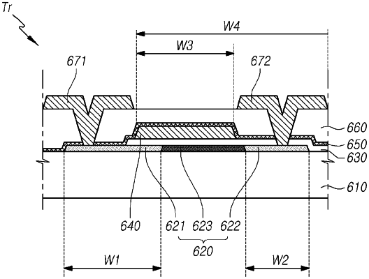
a first active layer disposed on the substrate, the first active layer including a first area, a second area spaced apart from the first area, and a channel area provided between the first area and the second area, wherein the first active layer is an oxide semiconductor and each of the first area and the second area of the first active layer is conductorized area, and wherein an electric resistance of each of the first area and the second area is lower than an electric resistance of the channel area;
a gate insulating film disposed on the first active layer;
a gate electrode of the at least one transistor disposed on the gate insulating film and overlapping a portion of the channel area of the first active layer;
an interlayer insulating film disposed on the gate electrode; and
a first electrode and a second electrode of the at least one transistor disposed on the interlayer insulating film and spaced apart from each other,
wherein the gate electrode overlaps a portion of at least one area of the first area and the second area of the first active layer.
|