| CPC H01L 27/1229 (2013.01) [H01L 27/1225 (2013.01); H01L 27/1251 (2013.01); H01L 27/1255 (2013.01); H01L 27/1259 (2013.01); H10K 59/1213 (2023.02)] | 13 Claims |
|
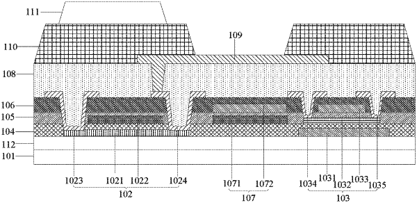
1. A display substrate, comprising:
a base substrate comprising a first area and a second area;
a low temperature poly-silicon transistor arranged in the first area; and
an oxide transistor arranged in the second area;
wherein the first area and the second area are not overlapped with each other;
the low temperature poly-silicon transistor comprises a poly-silicon active layer;
the oxide transistor comprises a first gate electrode;
the first gate electrode is arranged in a same layer as the poly-silicon active layer; and
a material of the first gate electrode is heavily-doped poly-silicon;
wherein the low temperature poly-silicon transistor further comprises: a second gate electrode, a first source electrode, and a first drain electrode;
wherein the second gate electrode, the first source electrode, and the first drain electrode are sequentially disposed on a side, facing away from the base substrate, of a layer where the poly-silicon active layer is located;
the first source electrode and the first drain electrode are electrically connected with the poly-silicon active layer; and
the oxide transistor further comprises: an oxide active layer, arranged between a layer where the second gate electrode is located and a layer where the first source electrode and the first drain electrode are located;
a third gate electrode, arranged between the oxide active layer and the layer where the first source electrode and the first drain electrode are located; and
a second source electrode and a second drain electrode, which are arranged in a same layer as the layer where the first source electrode and the first drain electrode are located;
wherein the second source electrode and the second drain electrode are electrically connected with the oxide active layer.
|