| CPC H01L 27/11807 (2013.01) [H01L 23/481 (2013.01); H01L 27/0207 (2013.01); H01L 2027/11829 (2013.01); H01L 2027/11864 (2013.01); H01L 2027/11881 (2013.01)] | 13 Claims |
|
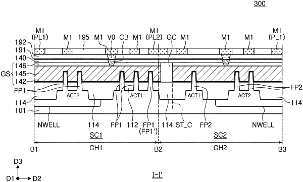
1. A semiconductor device comprising:
a first standard cell disposed on a substrate in a first row, the first standard cell having a first cell height;
a second standard cell disposed on the substrate in a second row adjacent to the first row, the second standard cell having a second cell height different from the first cell height; and
a power line extending in a first direction along a boundary between the first standard cell and the second standard cell,
wherein the first standard cell comprises:
a first base active region defined by a device isolation layer; and
a plurality of first fin patterns disposed on the first base active region and extending in the first direction,
wherein the second standard cell comprises:
a second base active region defined by the device isolation layer; and
a plurality of second fin patterns disposed on the second base active region and extending in the first direction,
wherein the device isolation layer is disposed between the first base active region and the second base active region,
wherein a central line of the power line and a central line of the device isolation layer are offset in a second direction, perpendicular to the first direction, the central line of the power line and the central line of the device isolation layer extending in the first direction,
wherein the plurality of first fin patterns comprises a first external fin pattern overlapping the power line in a vertical direction, and
wherein the first external fin pattern is disposed at the boundary between the first standard cell and the second standard cell.
|