| CPC H01L 27/0676 (2013.01) [H01L 21/2253 (2013.01); H01L 21/2254 (2013.01); H01L 21/26513 (2013.01); H01L 23/66 (2013.01); H01L 27/0814 (2013.01); H01L 29/868 (2013.01); H01L 21/822 (2013.01); H01L 29/6609 (2013.01); H01L 2223/6627 (2013.01); H01L 2223/6666 (2013.01); H01L 2223/6683 (2013.01)] | 20 Claims |
|
1. A method of manufacture of a monolithic diode limiter semiconductor structure, comprising:
providing an N-type semiconductor substrate;
providing an intrinsic layer on the N-type semiconductor substrate;
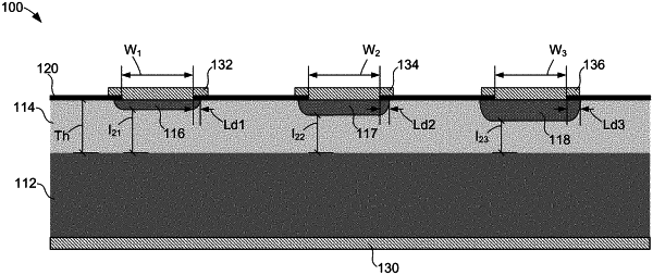
implanting a first P-type region to a first depth into the intrinsic layer to form a first PIN diode comprising a first effective intrinsic region of a first thickness;
implanting a second P-type region to a second depth into the intrinsic layer to form a second PIN diode comprising a second effective intrinsic region of a second thickness; and
forming at least one blocking capacitor and at least one inductor over the intrinsic layer.
|